![]({"xsmall":"https://www.zeiss.co.jp/content/dam/rms/countries/singapore/apac/lowkv-circles.png/_jcr_content/renditions/original.image_file.100.100.file/lowkv-circles.png","small":"https://www.zeiss.co.jp/content/dam/rms/countries/singapore/apac/lowkv-circles.png/_jcr_content/renditions/original.image_file.360.360.file/lowkv-circles.png","medium":"https://www.zeiss.co.jp/content/dam/rms/countries/singapore/apac/lowkv-circles.png/_jcr_content/renditions/original.image_file.768.768.file/lowkv-circles.png","large":"https://www.zeiss.co.jp/content/dam/rms/countries/singapore/apac/lowkv-circles.png/_jcr_content/renditions/original.image_file.1024.1024.file/lowkv-circles.png","xlarge":"https://www.zeiss.co.jp/content/dam/rms/countries/singapore/apac/lowkv-circles.png/_jcr_content/renditions/original./lowkv-circles.png","xxlarge":"https://www.zeiss.co.jp/content/dam/rms/countries/singapore/apac/lowkv-circles.png/_jcr_content/renditions/original./lowkv-circles.png","max":"https://www.zeiss.co.jp/content/dam/rms/countries/singapore/apac/lowkv-circles.png/_jcr_content/renditions/original./lowkv-circles.png"})
材料科学の研究者がZEISSのGeminiSEMをどのように使用しているか
電子顕微鏡の研究イノベーター
APAC地域の材料科学の世界を変えた最先端の優れた技術の電子顕微鏡であるZEISS GeminiSEMが30周年を迎えました。
Geminiカラムの技術の比類のない精度により新たな可能性を解き明かし、障壁を取り払ってきた一流の材料科学者の想像をかき立てる旅をご覧ください。
ZEISS GeminiSEMのコミュニティの一員となり、この分野の一流の人から学ぶための、このまたとない機会を逃さないでください。ZEISS GeminiSEMでご自身の研究を開始し、材料科学の将来を再定義してください!
ZEISS GeminiSEMの低加速電圧のイメージング技術とその技術が研究にどのように役立つか
![]({"xsmall":"https://www.zeiss.co.jp/content/dam/rms/countries/singapore/apac/lowkv11.png/_jcr_content/renditions/original.image_file.100.100.file/lowkv11.png","small":"https://www.zeiss.co.jp/content/dam/rms/countries/singapore/apac/lowkv11.png/_jcr_content/renditions/original.image_file.360.360.file/lowkv11.png","medium":"https://www.zeiss.co.jp/content/dam/rms/countries/singapore/apac/lowkv11.png/_jcr_content/renditions/original.image_file.768.768.file/lowkv11.png","large":"https://www.zeiss.co.jp/content/dam/rms/countries/singapore/apac/lowkv11.png/_jcr_content/renditions/original.image_file.1024.1024.file/lowkv11.png","xlarge":"https://www.zeiss.co.jp/content/dam/rms/countries/singapore/apac/lowkv11.png/_jcr_content/renditions/original./lowkv11.png","xxlarge":"https://www.zeiss.co.jp/content/dam/rms/countries/singapore/apac/lowkv11.png/_jcr_content/renditions/original./lowkv11.png","max":"https://www.zeiss.co.jp/content/dam/rms/countries/singapore/apac/lowkv11.png/_jcr_content/renditions/original./lowkv11.png"})
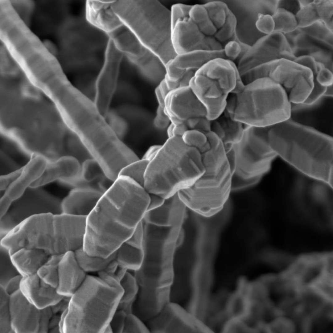
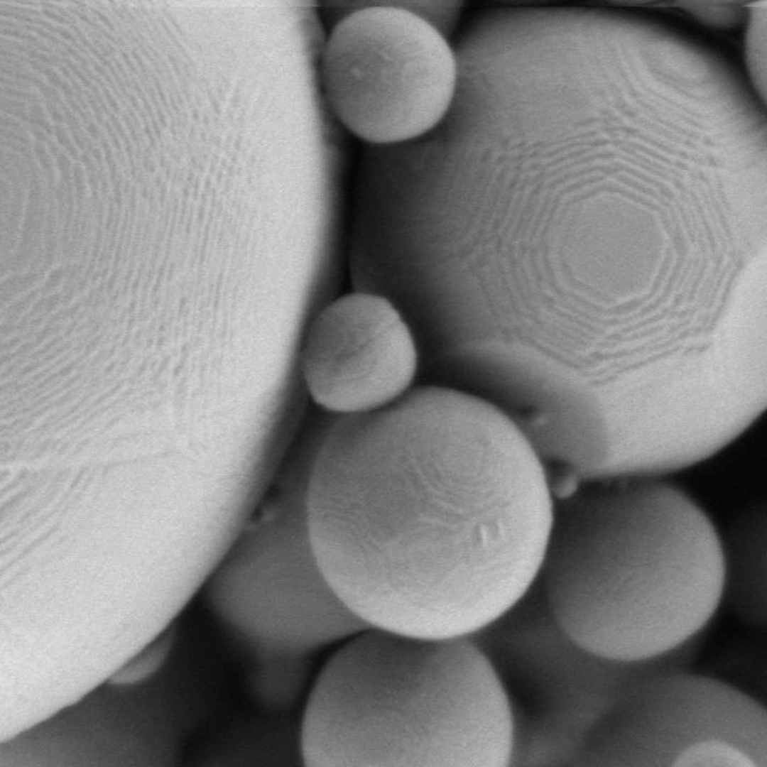
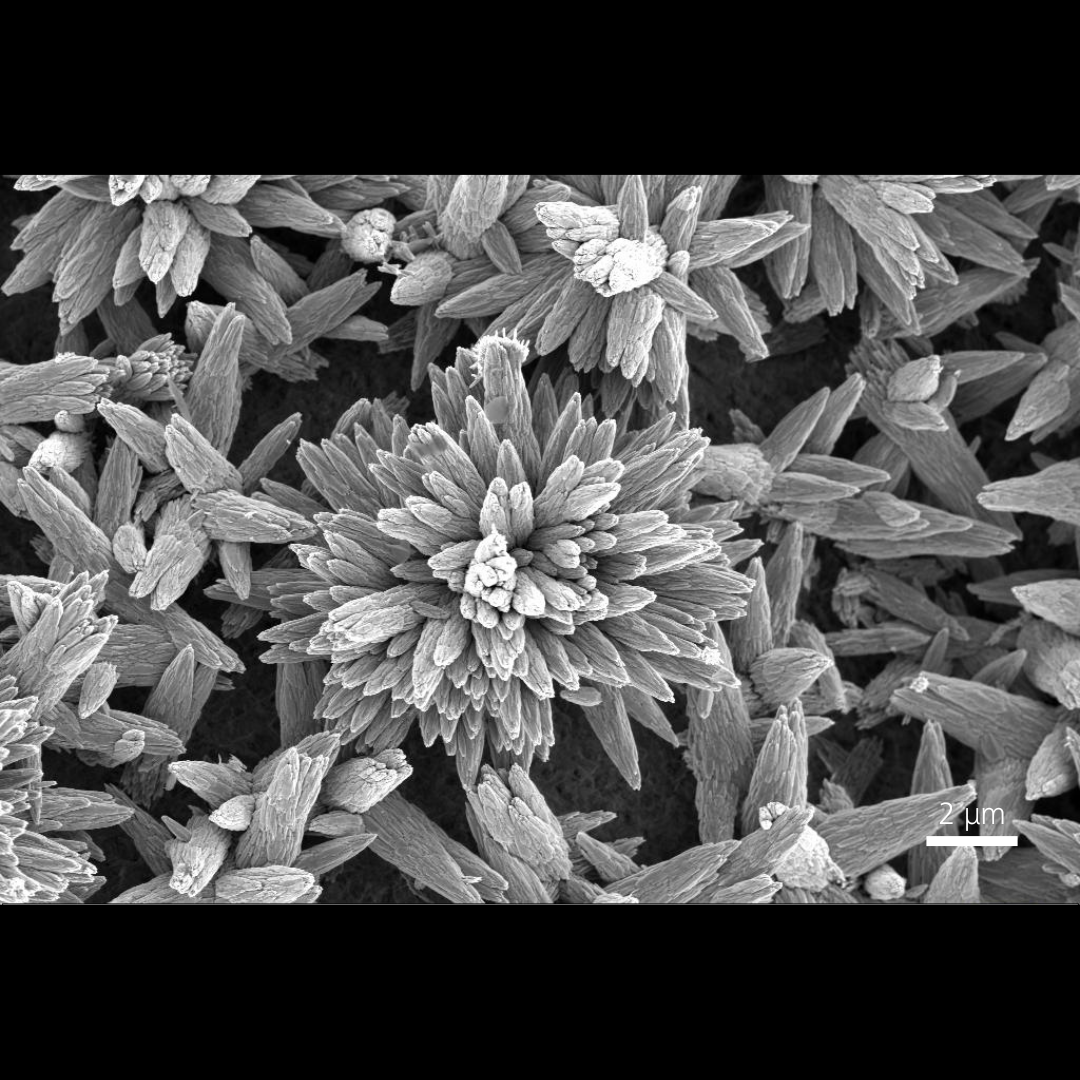
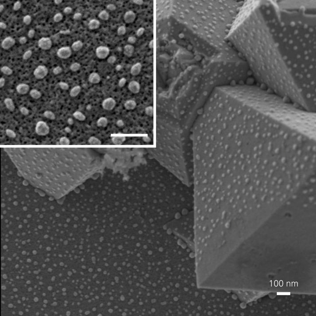
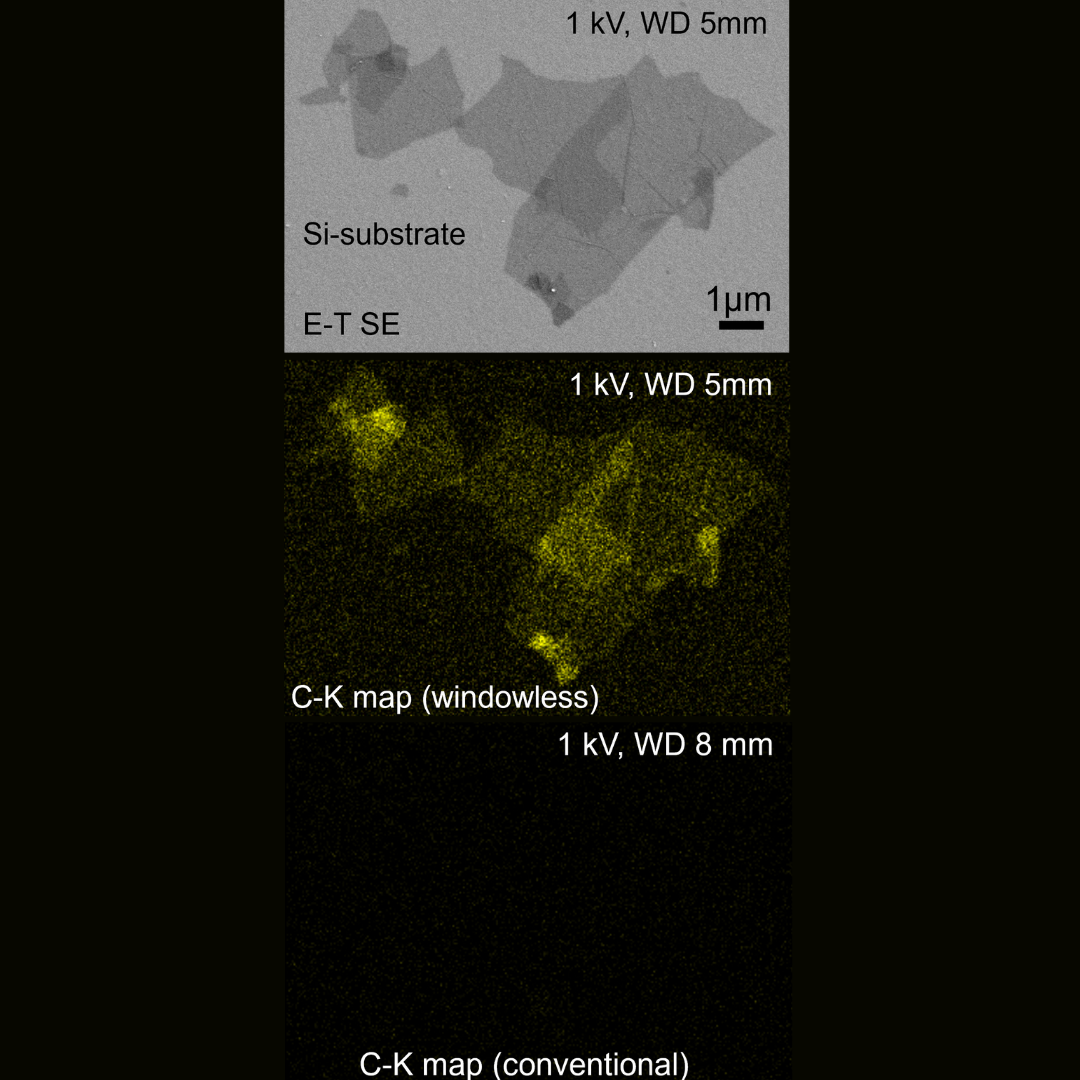
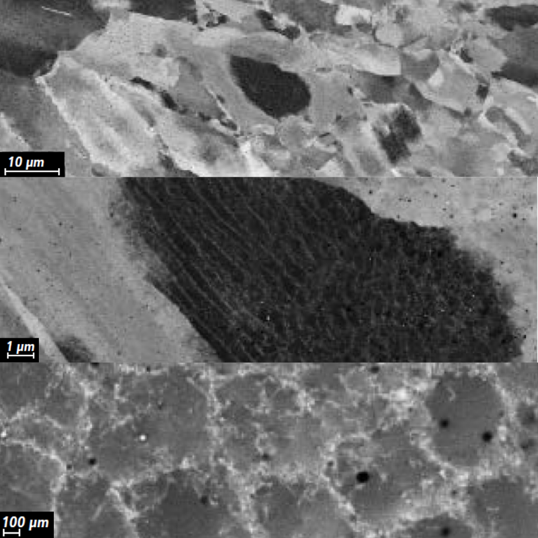
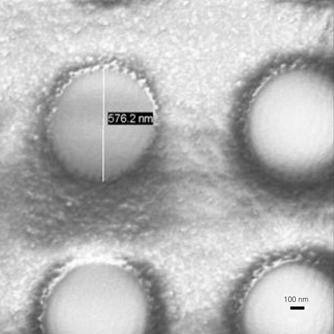
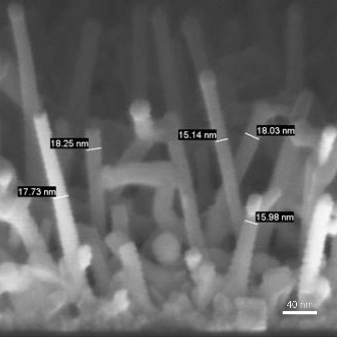
超低加速電圧で試料の真の表面イメージングを達成
メソポーラスシリカ、SiC繊維およびCNT等の非導電性の試料が、どのようにして高倍率の画像で高分解能を実現するかをご覧ください。試料は表面コーティングまたはステージバイアスなしで、0.5 kVから1 kVで撮像されました。
アジア太平洋地域の他の研究者が、どのようにZEISS GeminiSEMを使用しているか
ZEISSの電界放出型走査電子顕微鏡が、ユーザーや組織にもたらす恩恵を、中国、日本、韓国、インドおよび台湾からの異なる経歴を持つイノベーターが紹介します。
![Dr. Mario Hentschel Dr. Mario Hentschel]({"xsmall":"https://www.zeiss.co.jp/content/dam/rms/countries/singapore/apac/china-gemini41.jpg/_jcr_content/renditions/original.image_file.100.100.0,175,1049,1224.file/china-gemini41.jpg","small":"https://www.zeiss.co.jp/content/dam/rms/countries/singapore/apac/china-gemini41.jpg/_jcr_content/renditions/original.image_file.360.360.0,175,1049,1224.file/china-gemini41.jpg","medium":"https://www.zeiss.co.jp/content/dam/rms/countries/singapore/apac/china-gemini41.jpg/_jcr_content/renditions/original.image_file.768.768.0,175,1049,1224.file/china-gemini41.jpg","large":"https://www.zeiss.co.jp/content/dam/rms/countries/singapore/apac/china-gemini41.jpg/_jcr_content/renditions/original.image_file.1024.1024.0,175,1049,1224.file/china-gemini41.jpg","xlarge":"https://www.zeiss.co.jp/content/dam/rms/countries/singapore/apac/china-gemini41.jpg/_jcr_content/renditions/original.image_file.1049.1049.0,175,1049,1224.file/china-gemini41.jpg","xxlarge":"https://www.zeiss.co.jp/content/dam/rms/countries/singapore/apac/china-gemini41.jpg/_jcr_content/renditions/original.image_file.1049.1049.0,175,1049,1224.file/china-gemini41.jpg","max":"https://www.zeiss.co.jp/content/dam/rms/countries/singapore/apac/china-gemini41.jpg/_jcr_content/renditions/original.image_file.1049.1049.0,175,1049,1224.file/china-gemini41.jpg"})
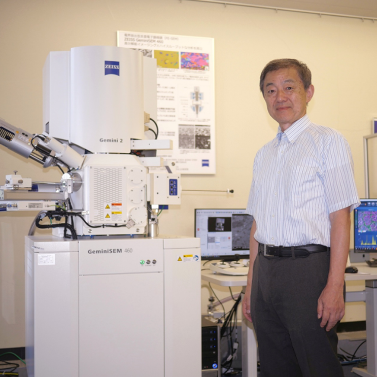
Ming博士は、国家自然科学基金、国家傑出青年科学基金プロジェクト、国家重点研究開発計画の50以上の重大プロジェクトの役目を果たすために、ZEISS GeminiSEMを使用しています。
![]({"xsmall":"https://www.zeiss.co.jp/content/dam/rms/countries/singapore/apac/kkt-korea30year4243.jpg/_jcr_content/renditions/original.image_file.100.100.1247,800,2651,2204.file/kkt-korea30year4243.jpg","small":"https://www.zeiss.co.jp/content/dam/rms/countries/singapore/apac/kkt-korea30year4243.jpg/_jcr_content/renditions/original.image_file.360.360.1247,800,2651,2204.file/kkt-korea30year4243.jpg","medium":"https://www.zeiss.co.jp/content/dam/rms/countries/singapore/apac/kkt-korea30year4243.jpg/_jcr_content/renditions/original.image_file.768.768.1247,800,2651,2204.file/kkt-korea30year4243.jpg","large":"https://www.zeiss.co.jp/content/dam/rms/countries/singapore/apac/kkt-korea30year4243.jpg/_jcr_content/renditions/original.image_file.1024.1024.1247,800,2651,2204.file/kkt-korea30year4243.jpg","xlarge":"https://www.zeiss.co.jp/content/dam/rms/countries/singapore/apac/kkt-korea30year4243.jpg/_jcr_content/renditions/original.image_file.1280.1280.1247,800,2651,2204.file/kkt-korea30year4243.jpg","xxlarge":"https://www.zeiss.co.jp/content/dam/rms/countries/singapore/apac/kkt-korea30year4243.jpg/_jcr_content/renditions/original.image_file.1404.1404.1247,800,2651,2204.file/kkt-korea30year4243.jpg","max":"https://www.zeiss.co.jp/content/dam/rms/countries/singapore/apac/kkt-korea30year4243.jpg/_jcr_content/renditions/original.image_file.1404.1404.1247,800,2651,2204.file/kkt-korea30year4243.jpg"})
Jeon博士は、現在、多様なお客様(産業界および学界)からの依頼で、ナノマテリアル/コンポーネント、セラミック、金属、高分子化合物、バイオまたは半導体等の様々な種類のサンプルを研究しています。
![]({"xsmall":"https://www.zeiss.co.jp/content/dam/rms/countries/singapore/apac/jaekim2.jpg/_jcr_content/renditions/original.image_file.100.100.100,234,930,1064.file/jaekim2.jpg","small":"https://www.zeiss.co.jp/content/dam/rms/countries/singapore/apac/jaekim2.jpg/_jcr_content/renditions/original.image_file.360.360.100,234,930,1064.file/jaekim2.jpg","medium":"https://www.zeiss.co.jp/content/dam/rms/countries/singapore/apac/jaekim2.jpg/_jcr_content/renditions/original.image_file.768.768.100,234,930,1064.file/jaekim2.jpg","large":"https://www.zeiss.co.jp/content/dam/rms/countries/singapore/apac/jaekim2.jpg/_jcr_content/renditions/original.image_file.830.830.100,234,930,1064.file/jaekim2.jpg","xlarge":"https://www.zeiss.co.jp/content/dam/rms/countries/singapore/apac/jaekim2.jpg/_jcr_content/renditions/original.image_file.830.830.100,234,930,1064.file/jaekim2.jpg","xxlarge":"https://www.zeiss.co.jp/content/dam/rms/countries/singapore/apac/jaekim2.jpg/_jcr_content/renditions/original.image_file.830.830.100,234,930,1064.file/jaekim2.jpg","max":"https://www.zeiss.co.jp/content/dam/rms/countries/singapore/apac/jaekim2.jpg/_jcr_content/renditions/original.image_file.830.830.100,234,930,1064.file/jaekim2.jpg"})
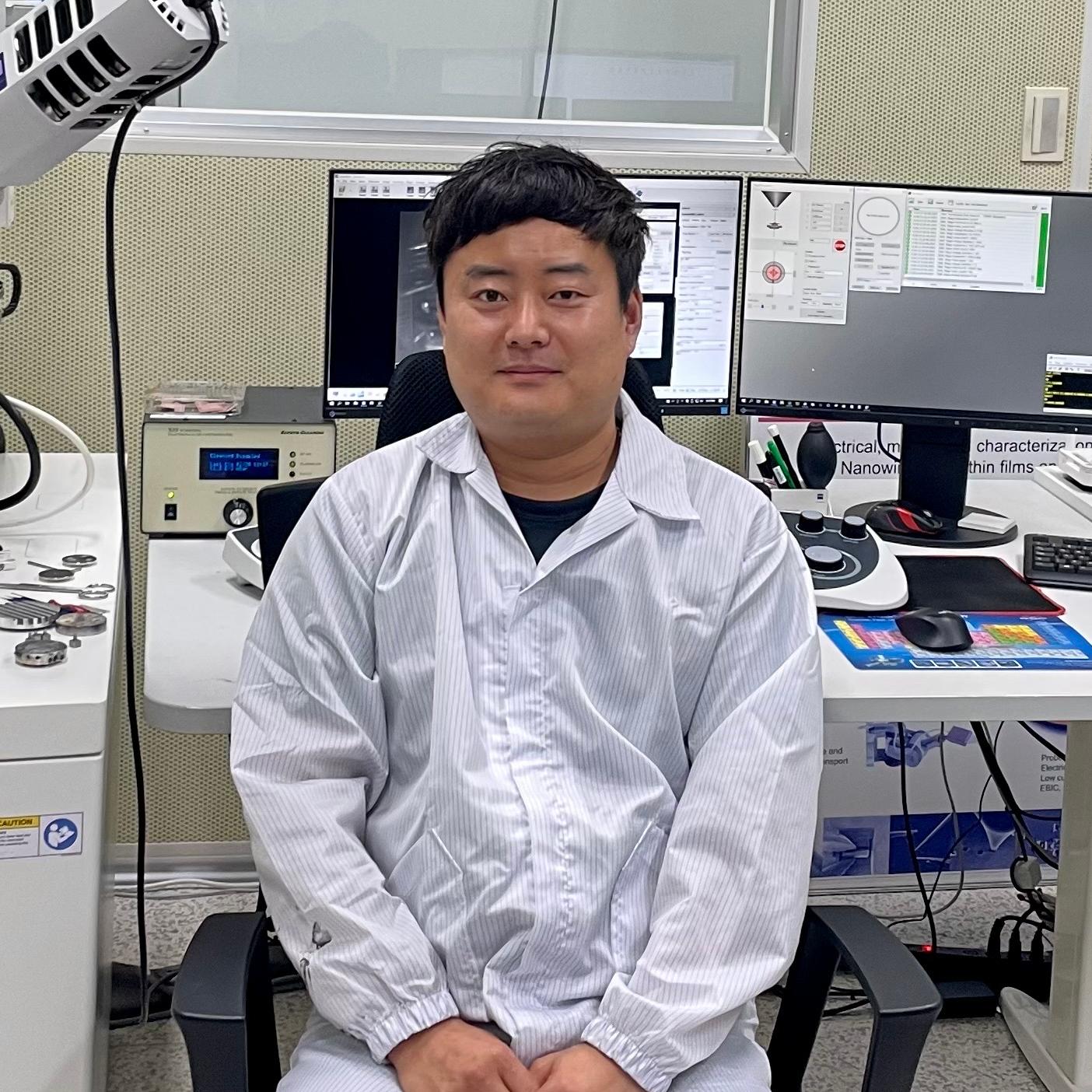
Kim博士は、現在、走査電子顕微鏡を使用して材料の特性を研究しています。博士は、特に3Dプリンティング関連の高分子材料、金属粉末および複合材料のイメージングに重点的に取り組んでいます。
![]({"xsmall":"https://www.zeiss.co.jp/content/dam/rms/countries/singapore/apac/liu-wen.jpg/_jcr_content/renditions/original.image_file.100.100.128,0,896,768.file/liu-wen.jpg","small":"https://www.zeiss.co.jp/content/dam/rms/countries/singapore/apac/liu-wen.jpg/_jcr_content/renditions/original.image_file.360.360.128,0,896,768.file/liu-wen.jpg","medium":"https://www.zeiss.co.jp/content/dam/rms/countries/singapore/apac/liu-wen.jpg/_jcr_content/renditions/original.image_file.768.768.128,0,896,768.file/liu-wen.jpg","large":"https://www.zeiss.co.jp/content/dam/rms/countries/singapore/apac/liu-wen.jpg/_jcr_content/renditions/original.image_file.768.768.128,0,896,768.file/liu-wen.jpg","xlarge":"https://www.zeiss.co.jp/content/dam/rms/countries/singapore/apac/liu-wen.jpg/_jcr_content/renditions/original.image_file.768.768.128,0,896,768.file/liu-wen.jpg","xxlarge":"https://www.zeiss.co.jp/content/dam/rms/countries/singapore/apac/liu-wen.jpg/_jcr_content/renditions/original.image_file.768.768.128,0,896,768.file/liu-wen.jpg","max":"https://www.zeiss.co.jp/content/dam/rms/countries/singapore/apac/liu-wen.jpg/_jcr_content/renditions/original.image_file.768.768.128,0,896,768.file/liu-wen.jpg"})
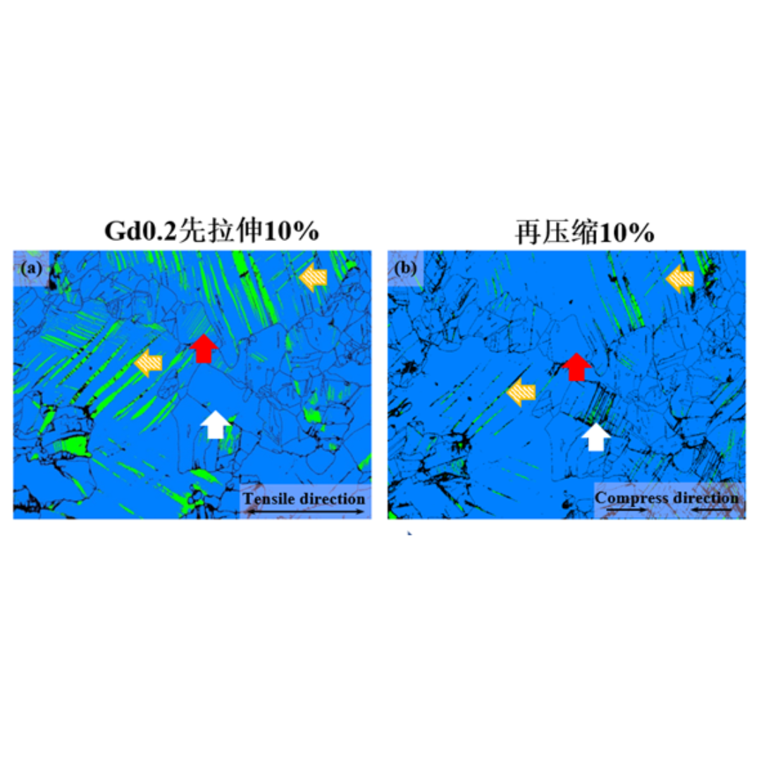
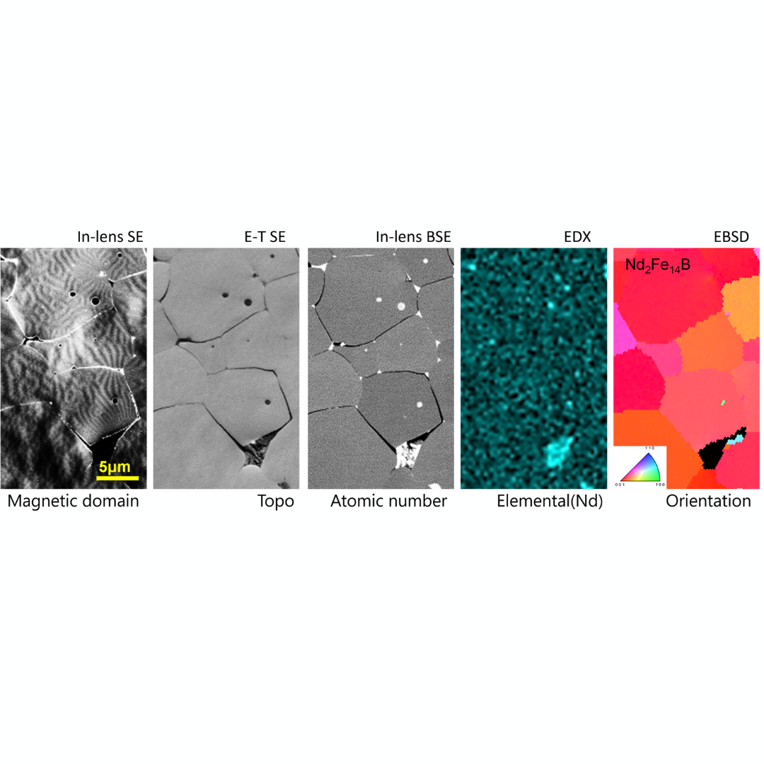
Chang博士は、非破壊でエピ層の微細構造の情報を提供するために、EBSD、ECP、ECCI等のSEMベースの技術を使用して、金属と化合物半導体のエレクトロエピタキシーを研究しています。
![]({"xsmall":"https://www.zeiss.co.jp/content/dam/rms/countries/singapore/apac/japansato.png/_jcr_content/renditions/original.image_file.100.100.111,0,854,743.file/japansato.png","small":"https://www.zeiss.co.jp/content/dam/rms/countries/singapore/apac/japansato.png/_jcr_content/renditions/original.image_file.360.360.111,0,854,743.file/japansato.png","medium":"https://www.zeiss.co.jp/content/dam/rms/countries/singapore/apac/japansato.png/_jcr_content/renditions/original.image_file.743.743.111,0,854,743.file/japansato.png","large":"https://www.zeiss.co.jp/content/dam/rms/countries/singapore/apac/japansato.png/_jcr_content/renditions/original.image_file.743.743.111,0,854,743.file/japansato.png","xlarge":"https://www.zeiss.co.jp/content/dam/rms/countries/singapore/apac/japansato.png/_jcr_content/renditions/original.image_file.743.743.111,0,854,743.file/japansato.png","xxlarge":"https://www.zeiss.co.jp/content/dam/rms/countries/singapore/apac/japansato.png/_jcr_content/renditions/original.image_file.743.743.111,0,854,743.file/japansato.png","max":"https://www.zeiss.co.jp/content/dam/rms/countries/singapore/apac/japansato.png/_jcr_content/renditions/original.image_file.743.743.111,0,854,743.file/japansato.png"})
佐藤博士は2000年以来ZEISS GeminiSEMのユーザーです。触媒、電池、磁石、新合金などの様々な先端材料の研究にGeminiSEMを活用しています。博士の「スイートスポットイメージング」による条件最適化は、研究者達が新しい視点で走査電子顕微鏡を使うヒントを与えています。
![]({"xsmall":"https://www.zeiss.co.jp/content/dam/rms/countries/singapore/apac/india-testimonial17.png/_jcr_content/renditions/original.image_file.100.100.88,139,949,1000.file/india-testimonial17.png","small":"https://www.zeiss.co.jp/content/dam/rms/countries/singapore/apac/india-testimonial17.png/_jcr_content/renditions/original.image_file.360.360.88,139,949,1000.file/india-testimonial17.png","medium":"https://www.zeiss.co.jp/content/dam/rms/countries/singapore/apac/india-testimonial17.png/_jcr_content/renditions/original.image_file.768.768.88,139,949,1000.file/india-testimonial17.png","large":"https://www.zeiss.co.jp/content/dam/rms/countries/singapore/apac/india-testimonial17.png/_jcr_content/renditions/original.image_file.861.861.88,139,949,1000.file/india-testimonial17.png","xlarge":"https://www.zeiss.co.jp/content/dam/rms/countries/singapore/apac/india-testimonial17.png/_jcr_content/renditions/original.image_file.861.861.88,139,949,1000.file/india-testimonial17.png","xxlarge":"https://www.zeiss.co.jp/content/dam/rms/countries/singapore/apac/india-testimonial17.png/_jcr_content/renditions/original.image_file.861.861.88,139,949,1000.file/india-testimonial17.png","max":"https://www.zeiss.co.jp/content/dam/rms/countries/singapore/apac/india-testimonial17.png/_jcr_content/renditions/original.image_file.861.861.88,139,949,1000.file/india-testimonial17.png"})
Purakkat博士は、ZEISS GeminiSEMカラムを使用して、正確なコントラストと収差補正により50 nm以下の誘電性のフィルムを撮像しています。特に、博士は低加速電圧イメージングの際にカラムを使用しており、より鮮明ではっきりした画像を取得し、パターンのあるサンプルをより効果的に観察しています。
![]({"xsmall":"https://www.zeiss.co.jp/content/dam/rms/countries/singapore/apac/india-testimonial16.png/_jcr_content/renditions/original.image_file.100.100.0,0,691,691.file/india-testimonial16.png","small":"https://www.zeiss.co.jp/content/dam/rms/countries/singapore/apac/india-testimonial16.png/_jcr_content/renditions/original.image_file.360.360.0,0,691,691.file/india-testimonial16.png","medium":"https://www.zeiss.co.jp/content/dam/rms/countries/singapore/apac/india-testimonial16.png/_jcr_content/renditions/original.image_file.691.691.0,0,691,691.file/india-testimonial16.png","large":"https://www.zeiss.co.jp/content/dam/rms/countries/singapore/apac/india-testimonial16.png/_jcr_content/renditions/original.image_file.691.691.0,0,691,691.file/india-testimonial16.png","xlarge":"https://www.zeiss.co.jp/content/dam/rms/countries/singapore/apac/india-testimonial16.png/_jcr_content/renditions/original.image_file.691.691.0,0,691,691.file/india-testimonial16.png","xxlarge":"https://www.zeiss.co.jp/content/dam/rms/countries/singapore/apac/india-testimonial16.png/_jcr_content/renditions/original.image_file.691.691.0,0,691,691.file/india-testimonial16.png","max":"https://www.zeiss.co.jp/content/dam/rms/countries/singapore/apac/india-testimonial16.png/_jcr_content/renditions/original.image_file.691.691.0,0,691,691.file/india-testimonial16.png"})
Ruma博士は、ナノマテリアル、薄膜、金属/セラミック複合体および微生物細胞の形態、表面組成、次元解析の研究をしています。
![]({"xsmall":"https://www.zeiss.co.jp/content/dam/rms/countries/singapore/apac/gemini-suwas.jpg/_jcr_content/renditions/original.image_file.100.100.0,1,1495,1496.file/gemini-suwas.jpg","small":"https://www.zeiss.co.jp/content/dam/rms/countries/singapore/apac/gemini-suwas.jpg/_jcr_content/renditions/original.image_file.360.360.0,1,1495,1496.file/gemini-suwas.jpg","medium":"https://www.zeiss.co.jp/content/dam/rms/countries/singapore/apac/gemini-suwas.jpg/_jcr_content/renditions/original.image_file.768.768.0,1,1495,1496.file/gemini-suwas.jpg","large":"https://www.zeiss.co.jp/content/dam/rms/countries/singapore/apac/gemini-suwas.jpg/_jcr_content/renditions/original.image_file.1024.1024.0,1,1495,1496.file/gemini-suwas.jpg","xlarge":"https://www.zeiss.co.jp/content/dam/rms/countries/singapore/apac/gemini-suwas.jpg/_jcr_content/renditions/original.image_file.1280.1280.0,1,1495,1496.file/gemini-suwas.jpg","xxlarge":"https://www.zeiss.co.jp/content/dam/rms/countries/singapore/apac/gemini-suwas.jpg/_jcr_content/renditions/original.image_file.1440.1440.0,1,1495,1496.file/gemini-suwas.jpg","max":"https://www.zeiss.co.jp/content/dam/rms/countries/singapore/apac/gemini-suwas.jpg/_jcr_content/renditions/original.image_file.1495.1495.0,1,1495,1496.file/gemini-suwas.jpg"})
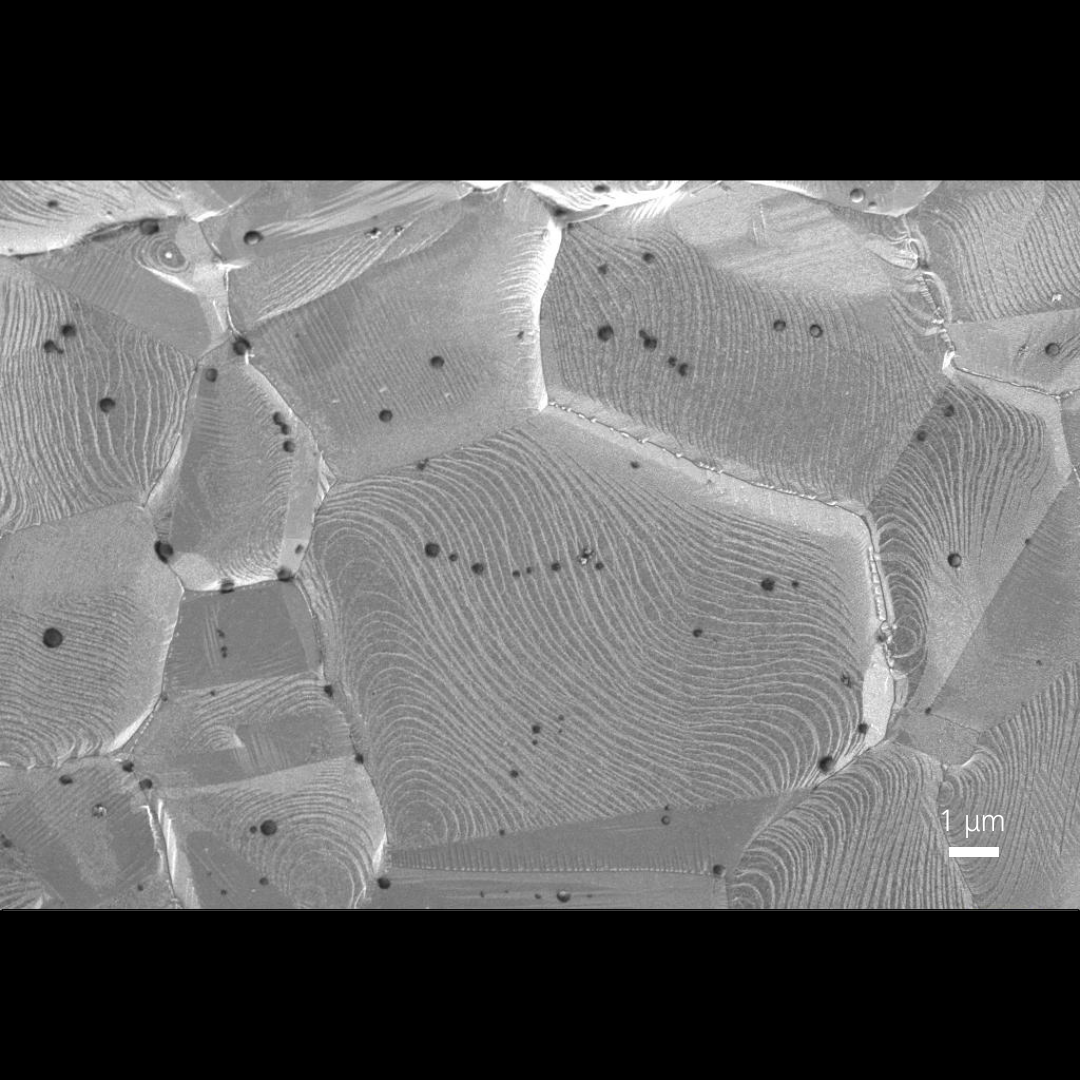
Suawas博士は、現在、変形やアニール処理された金属および合金を研究しています。
画像上の丸印をクリックして、詳細情報をご覧ください。
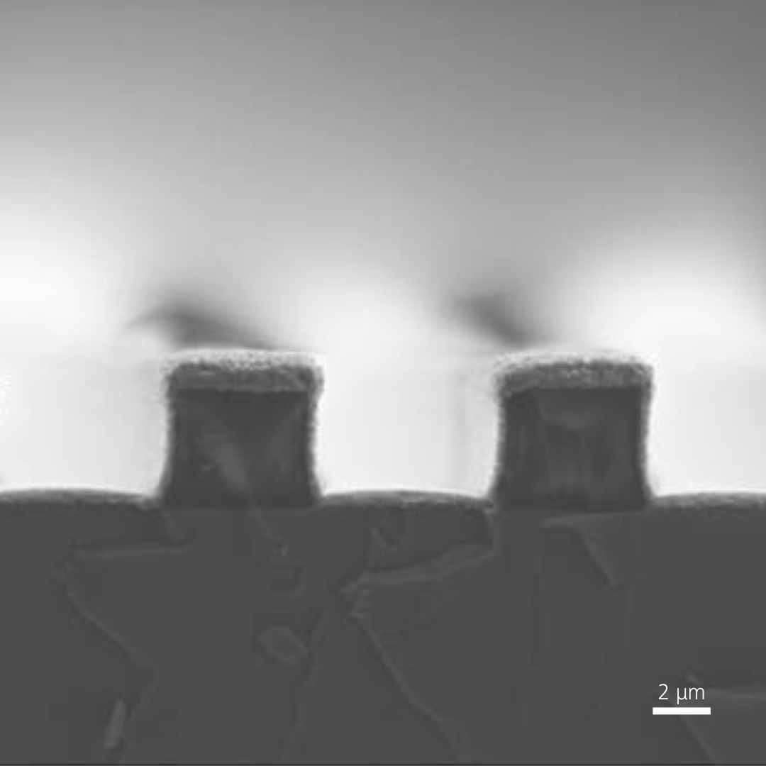
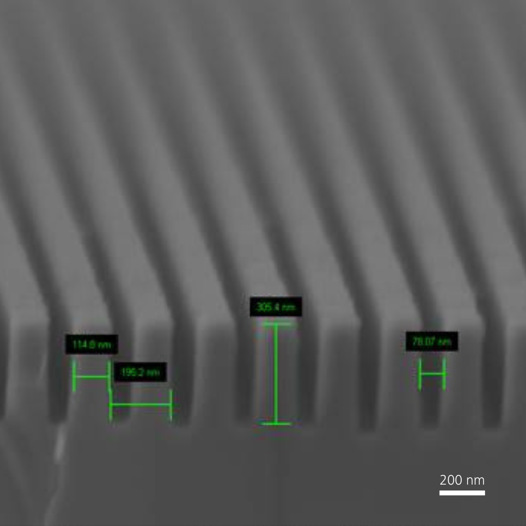
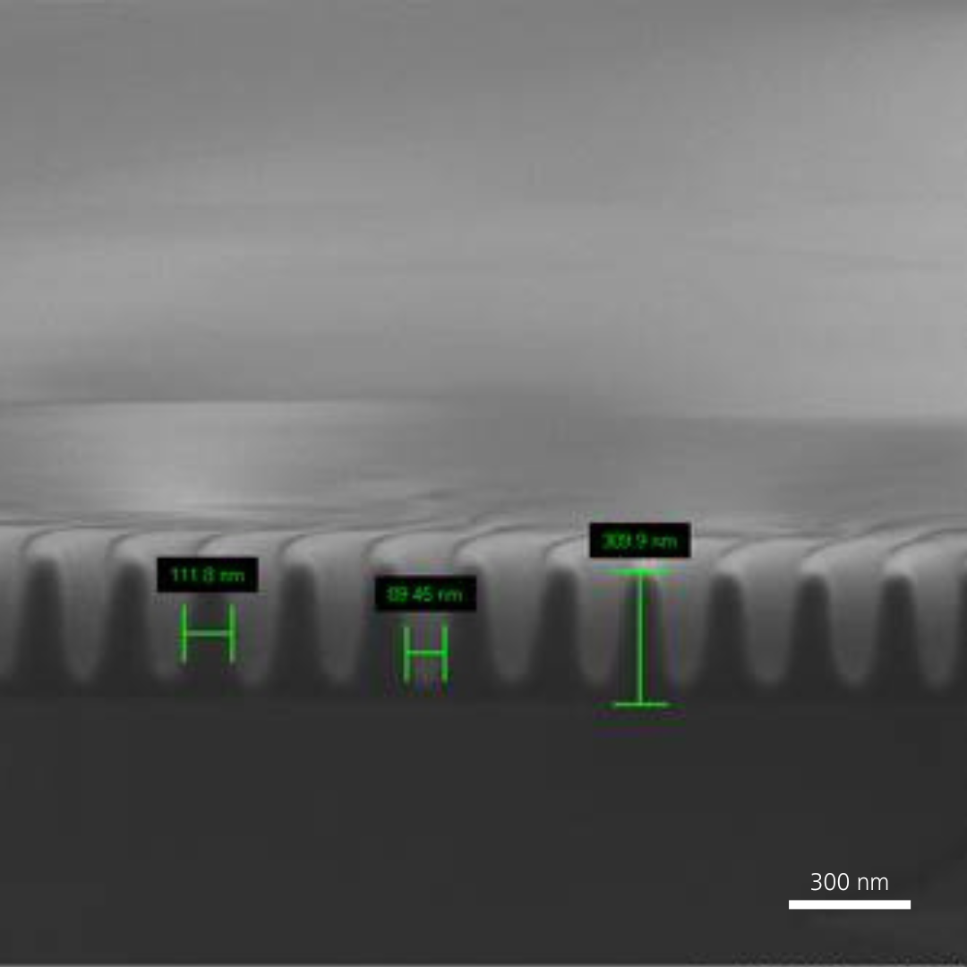
Gemini光学系を支える技術
グリッド電圧が検出用の二次電子または反射電子を選択することができます。
このレンズは、最適化された開き角によりビーム電流とスポットサイズを決めます。
EsB検出器は、最低加速電圧でも高い材料コントラストが可能で、フィルターグリッドにより、エネルギーに応じて反射電子の識別ができます。
ビームブースターは、一体型ビーム減速装置で、小さなプローブサイズと高いSN比を保証します。ブースターは、収差の抑制と外部磁場からの保護により、カラムを通過するビームをブーストし、ポールピースでビームを減速させることで、低加速電圧で最高の画質を実現します。
小スポットサイズ用の熱電界放出型電子銃
二次電子は試料表面から収集され、極めて高い分解能、表面感度及び独自なコントラストを実現します。
対物レンズがプローブの焦点をサンプルに合わせます。
静電レンズ(Geminiの対物レンズ)と共に、電子が集束され、極めて高い分解能を実現します。
ナノ粒子から大型機械のパーツまで、ほんの少しのサンプル調製でSEMでの観察が可能です。
磁界レンズ(Geminiの対物レンズ)と共に、電子が集束され、極めて高い分解能を実現します。
電子ビームを走査し、信号検出を同期させ、画像を形成します。